 HOME
HOME
 Shopping Cart
 User Center
 Product Category
Service Hotline
00864006988696
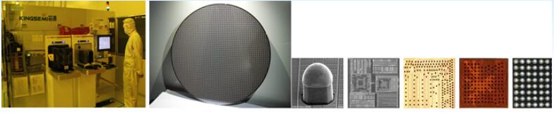
Production Overview
Wafer-level packaging (WLP) is the technology of packaging an integrated circuit while still part of the wafer, in contrast to the more conventional method of wire bonding. WLP is essentially a true chip-scale package (CSP) technology, since the resulting package is practically of the same size as the die.
TFME offers various leading edge wafer bumping processes. WLP is a wafer level packaging technology which uses cu pillar or solder bumps to form the interconnection between the integrated circuit (IC) and the motherboard (or Lead frame). WLP includes wafer bumping with or without Redistribution Layer (RDL), wafer level final test, wafer singulation and device packing in tape & reel to support full turn‑key solution. TFME’s Under Bump metallurgy (UBM) over PBO or PI layers on the die active surface provides a reliable interconnect solution to meet the demands of the growing global consumer market place for portable electronics.
TFME offers customers with both 200mm and 300mm WLP Layout Design, Qualify and Mass Production services, including plated solder bump/Cu Pillar bump and ball placement technology with lead free materials.
Application
The WLP package family is applicable for a wide range of semiconductor device types from high end AP/PA/BB/RFIC chips, to Wireless LAN, card, switch, power management, memory, and standard analog, etc.
Wafer Level Features
* 4-256 ball count
* Small body 0.64 mm2 to large 57.0 mm2 body size
* PBO, Polyimide (PI) & LCP (low curing temperature polymer) Re-passivation and Re-distribution Layer (RDL) available
* Cu Pillar. Solder bump and SAC Alloy ball-loaded bumping options
* Reliable thick Cu RDL and Cu UBM with good electrical performance
* Compatible with conventional SMT assembly and test techniques
Die Level Features
* Best in package level and board level reliability
* Back-side lamination available
* Cost effective T&R packaging solutions for small ICs
* Full turnkey WLP, including probing and DPS
* Wide selection of pocket tape carrier options
Reliability Test Standards
The test criterion is zero defect out of 77 sampling units.
JEDEC Precondition MSL-1:J-STD-20/JESD22-A113
| Temp/Humidity Test | 85°C/ 85% RH, 1000hrs, JEDEC 22- A101 |
| Pressure Cooker Test | 121°C/ 100% RH/ 15 PSIG, 96hrs, JEDEC 22- A102 |
| Temp Cycle Test | -65 ~ 150°C, 500cycles, JEDEC22-A104 |
| High Temp Storage Test | 150°C, 1000hrs, JEDEC 22- A103 |

Seller Info after you register

About us | Shopping guide | Business license | Help center | Links | Contact us
Copyright© Semiconductor mall 2015-2016,All Rights Reserved
JingICPPrepare15002921
