 HOME
HOME
 Shopping Cart
 User Center
 Product Category
Service Hotline
00864006988696
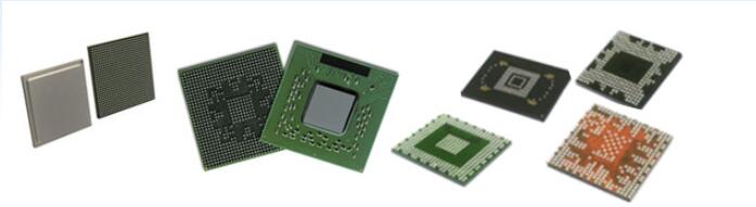
Production Overview
Flip Chip packaging, in which the silicon die is directly attached to the substrate in a face-down way using solder bumps or Cu pillar instead of wire bonds, provides the shortest electrical path with high electrical and thermal performance.
NFME offers customers with full turnkey process for Flip Chip product from Wafer Bumping, Wafer Probing, Flip Chip assembly, Final Test and System Level Test. The Flip Chip product portfolio includes FCBGA, FCBGA-H, FCCSP, FCLGA, FCQFN, and FCSOT, etc.
Application
The FC package family is applicable for a wide range of semiconductor device types from high end AP/CPU/GPU/BB/RFIC chips, to Wireless LAN, network switch, power management, memory, and standard linear, analog etc.
Key Features
* SiP (FC+SMT+Wirebond) available.
* CUF, MUF available.
* Cu Pillar, Solder bump (LF) available.
* Various substrate technology qualified including SAP, MSAP, ETS, MIS and SLP.
* Fully Turnkey for wafer bumping, probing, assembly, FT and SLT available.
Reliability Test Standards
The test criterion is zero defect out of 77 sampling units.
JEDEC Precondition:J-STD-20/JESD22-A113
|
TCT |
-55 ~ 125°C, 500/1000cycles, JEDEC22-A104 |
|
U-HAST |
130℃/85%RH,33.5 PSI,96/192hr, JEDEC 22-A118 |
|
HTST |
150°C, 1000hrs, JEDEC 22- A103 |
|
|
|
MUF FCCSP Design Rule
|
Die Thk |
Min 80um |
Mold Cap Thk |
0.25-0.65mm |
|
Substrate Thk |
Min 0.11mm |
SMT Capacitor |
Min 01005 |
|
BP |
79um |
S/B Size |
Min 0.20mm |
|
BD |
30um |
S/B Pitch |
Min 0.35mm |
|
Gap Height |
Min 40um |
Surface Surface |
Ni/Au, OSP, IT |
Seller Info after you register

About us | Shopping guide | Business license | Help center | Links | Contact us
Copyright© Semiconductor mall 2015-2016,All Rights Reserved
JingICPPrepare15002921
