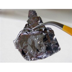
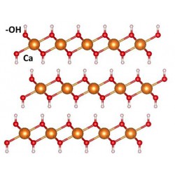
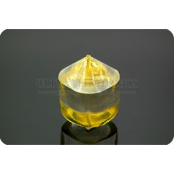
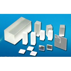
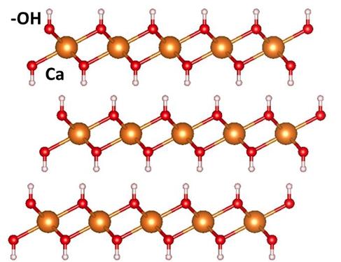
Ca(OH)2 Crystal
Ca(OH)2 crystal was obtained by hydrothermal synthesis.
Product summary:
L Spatial Group: P-3m1
L Layering: Yes/Can be peeled to a single layer
L Band Gap: [4.0 eV]
L Purity: Semiconductor grade (5.5N) 99.9995%
Growth Technology: Gas Phase Transport - Duration: 2 Months
Sample size: [5 mm]
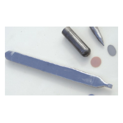
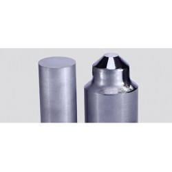
Mg(OH) rammed crystal
Mg (OH) rammed crystals were obtained by hydrothermal synthesis.
Product summary:
L Spatial Group: P-3m1
L Layering: Yes/Can be peeled to a single layer
L Band Gap: [4.0 eV]
L Purity: Semiconductor grade (6N) 99.9999%
Growth technology: hydrothermal synthesis under 45 MPa pressure for 1.5 months
Sample size: [10 mm]
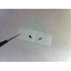
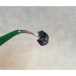
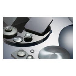
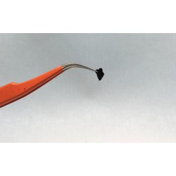
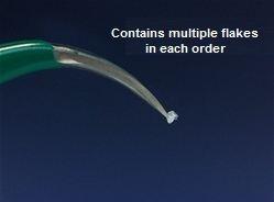
H-BN powder
The economic stripping solution is h-BN. The h-BN powder (see figure) can be used many times (+10,000 times) and peeled onto any substrate. The microcrystals are used for conventional peeling and liquid phase peeling.
The half peak width (FWHM) of hBN thin films is larger than 6-7 cm-1, which is in good agreement with the published data.
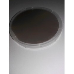
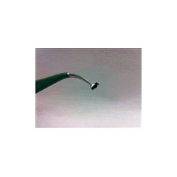
H-BN crystal
The size of h-BN crystal can reach 2mm, which is regarded as the gold standard in the field of two-dimensional materials. The defect-free h-BN sheet is the only commercially available two-dimensional semi-insulating material for high performance two-dimensional electronic and photonic devices.
Hexagonal boron nitride (h-BN) single crystal is an ideal two-dimensional substrate material. The Raman spectra show that the half peak width (FWHM) at 1566 cm-1 is less than 5 cm-1, indicating its high crystallinity. The bandgap is 5.2 eV and is considered as a wide bandgap semiconductor/insulator. It has chemical inertia, atomic plane.
Application:
L Electronic Products
L Sensor-Detector
L STM-AFM Application
L Study of Ultra-Low Friction (Tribology)
L Materials Science and Semiconductor Research
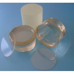
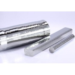
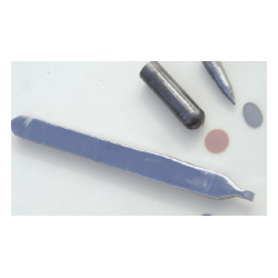
Mica sheet
MICA Ca
Product des
cription
Members of the stratiform mica family whose chemical formulas have been adjusted are rich in K, Mg and Fe, giving them ideal co
nductivity and charged surface (Chemically identified as Al 2 Ca (AlSi) 2O10 (OH) 2). The product can be synthesized by hydrothermal method within one month. Stripping completely in the direction of C lattice. The purity of the product is 99.9998%. ba
sed on absorption measurement, the edge of subband appears at 4.8 eV. Crystal symmetry is C 2/m, C m (monoclinic) layered material. The crystal size is over 1 cm and can be preserved for many years.
MICA Ca/Mg
Product des
cription
Members of the stratiform mica family whose chemical formulas have been adjusted are rich in Ca and Mg, giving them ideal co
nductivity and charged surface (chemical formulas identified as Ca (Al, Mg) 3 (SiAl3) O10 (OH) 2). The product can be synthesized by hydrothermal method within one month. Arranged in the direction of C lattice as a layered structure, easy to peel off. The purity of the product is 99.9998%. ba
sed on absorption measurement, the edge of subband appears at 3.5 eV. Crystal symmetry is C 2/m, C m (monoclinic) layered material. The crystal size is over 1 cm and can be preserved for many years.
MICA K/Li
Product des
cription
Members of the stratiform mica family whose chemical formulas have been adjusted are rich in K and Li, giving them ideal co
nductivity and 4 O 10 (F, OH) of charged surface (Al, Si) of K (LiAlRb) 3). The product was synthesized by hydrothermal method within one month. The purity of the product is 99.9998%. ba
sed on absorption measurement, the band edge appears at 4.1 eV. Crystal symmetry is C 2/m, C m (monoclinic) layered material, easy to peel. The crystal size is over 1 cm and can be preserved for many years.
MICA K/Mg/Fe
Product des
cription
Members of the stratiform mica family whose chemical formulas have been adjusted are rich in K, Mg and Fe, giving them ideal co
nductivity and charged surface (identified as K (FeMg) 3Si3AlO10 (OH) 2). The product was synthesized by hydrothermal method in one month. The purity of the product is 99.9998%. ba
sed on absorption measurement, the band edge appears at 4.2 eV. Crystal symmetry is C 2/m, C m (monoclinic) layered material, easy to peel. The crystal size is over 1 cm and can be preserved for many years.
 Website Homepage
 Shopping cart
 User center
 Product Category
 inquiry experts