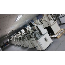
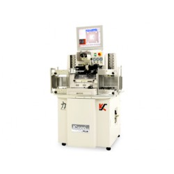
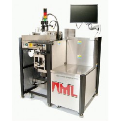
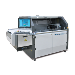
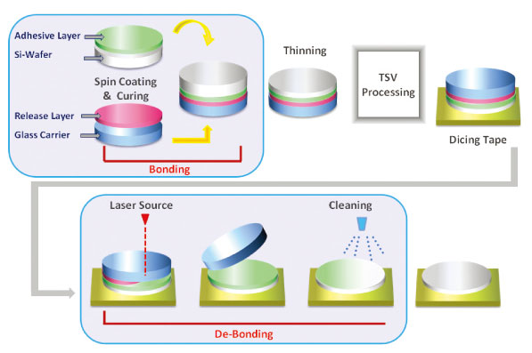
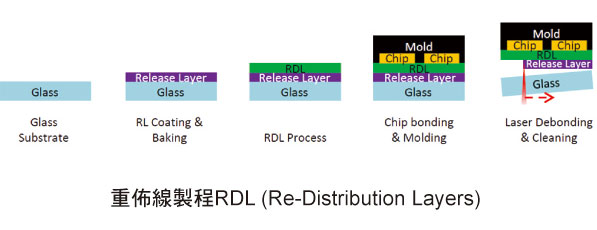
Wafer Laser De-bonding Equipment
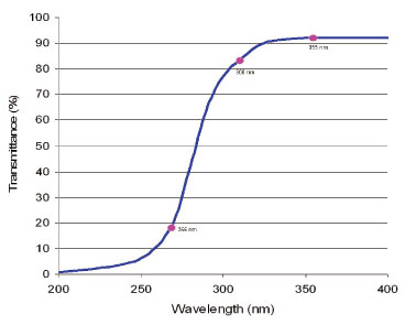
- IBM Patented High Efficiency Laser Stripping System, using 355 nm solid-state laser (solid-stale Lascr), using cold cutting, non-thermal effect, high-frequency fast scanning.
Laser with special peeling coating, special thin coating, high laser absorption, excellent chemical resistance, high temperature stability (350 C)
It can be used with various adhesives and adhesives on the market (suitable for high or low temperature).
Maintenance cost is low.
Low power laser to avoid damage to the wafer.
Suitable for 12 "wafer and square" fan-out wafer level packaging.
-
application
Semiconductor industry: 2.5D/3D IC, 35-family, communication wafer, fan-out wafer-level packaging
(Fan-Out Wafer Level Packaging ; FOWLP) IGBT/Power Device , Glass/Organic/Si Interposer
Photoelectric industry:Flexible OLED Dispaly, Thin Touch Sensor, Thin Glass Handling
(Fan-Out Wafer Level Packaging ; FOWLP)
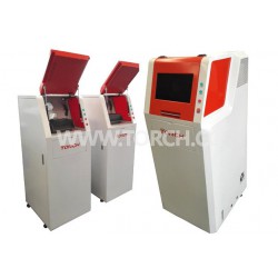
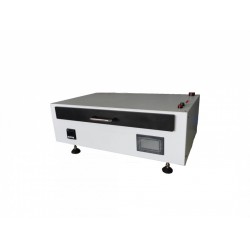
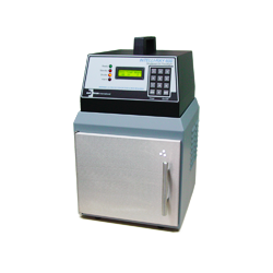
Wafer Cleaning Equipment
- Rapid cleaning of residue.
With a protective design of wafer cutting tape (Dicing Type), chemical damage can be avoided.
Fast parallel processing can clean multiple wafers at the same time.
Multimode design can solve the problem of slow output rate at this stage.
Chemicals can be recycled.
Energy-saving design.
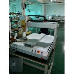
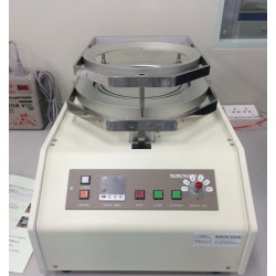
Wafer Bonding Equipment
Applicable to 8 ~ 12 "wafer, can quickly heat and cool, and uniform temperature control.
Special design of cooling and pressing control can control wafer warpage.
The arrangement of multiple bonding modules can process multiple wafers at the same time, and the output rate is faster.
It can be used in high temperature and low temperature processes.
Temperature and pressure data real-time monitoring, as well as closed-loop pressure compensation, can grasp and control the adjustment of real-time process changes.
application
2.5D/3D IC, back-illuminated photosensitive elements, three or five families, communication chips, S01 wafer correlation, micro-electromechanical system, Fan-Out Wafer Level Packaging; FOWLP)
 Website Homepage
 Shopping cart
 User center
 Product Category
 inquiry experts experts