 Website Homepage
 Shopping cart
 User center
 Product Category
 inquiry experts


Service Hotline
00864006988696


Negotiable

Negotiable

Negotiable
¥0.05

Negotiable
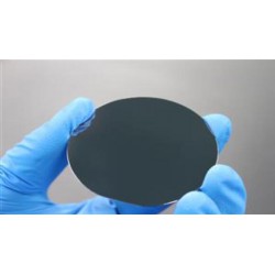
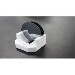
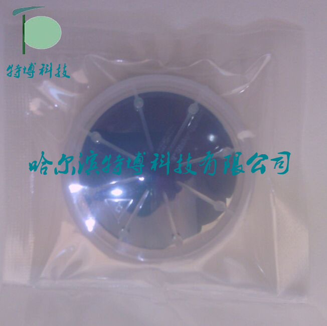
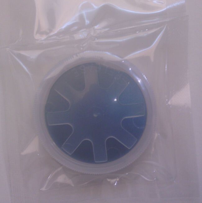
砷化镓(gallium arsenide),化学式GaAs,属Ⅲ-Ⅴ族化合物半导体,由砷和镓两种元素化合而成,外观呈亮灰色,具金属光泽、性脆而硬,是当代国际公认的继"硅(Silicon)"之后最成熟的化合物半导体材料,具有高频率、高电子迁移率、高输出功率、低噪音以及线性度良好等优越特性,是光电子和微电子工业最重要的支撑材料之一。
在光电子工业领域应用层面,砷化镓单晶可被用于制作LD(激光器)、LED(发光二极管)、光电集成电路(OEIC)、光伏器件等;
在微电子工业领域应用层面,可被用于制作MESFET(金属半导体场效应管)、HEMT(高电子迁移率晶体管)、HBT(异质结双极晶体管)、IC、微波二极管、Hall器件等。
主要涉及高端军事电子应用、光纤通信系统、宽带卫星无线通信系统、测试仪器、汽车电子、激光、照明等领域。作为重要的半导体材料,GaAs的电子迁移率为硅和氮化镓的5倍,用于中小功率微波器件具有更低的功率损耗,因此在手机通讯、局域无线网、GPS和汽车雷达等领域中占主导地位。
If you have any questions before purchasing, please contact us.

About us | Shopping guide | Business license | Help center | Links | Contact us
Copyright© Semiconductor mall 2015-2016,All Rights Reserved
JingICPPrepare15002921
