 Website Homepage
 Shopping cart
 User center
 Product Category
 inquiry experts


Service Hotline
00864006988696


Negotiable

Negotiable

Negotiable
¥0.05

Negotiable
| 分类/Category | 应用/Application | 说明/Description |
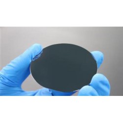
| InP基半导体光电外延片 InP based epiwafer |
FP laser | ~1310 nm/~1550 nm/~1650 nm/~2000 nm/~2300 nm |
| DFB laser | 1270-1630 nm/~2000 nm/~2300 nm | |
| Avalanche photodiode | 1250-1600 nm | |
| Photodiode | 1250-1600 nm/>2000 nm (InGaAs absorptive layer) <1400 nm (InGaAsP absorptive layer) |
|
| InAs/InP quantum dot laser | 1500-1850 nm | |
| InAs/InP quantum dot SOA | 1500-1850 nm |
If you have any questions before purchasing, please contact us.

About us | Shopping guide | Business license | Help center | Links | Contact us
Copyright© Semiconductor mall 2015-2016,All Rights Reserved
JingICPPrepare15002921
