 Website Homepage
 Shopping cart
 User center
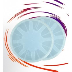
 Product Category
 inquiry experts


Service Hotline
00864006988696


Consumer Hotline:00864006988696
Negotiable

Negotiable

Negotiable
¥0.05

Negotiable
|
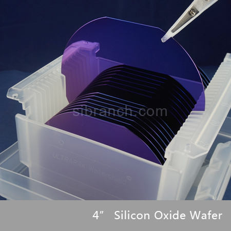
用 途 |
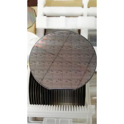
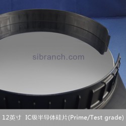
同步辐射样品载体、PVD/CVD镀膜做衬底、磁控溅射生长样品、XRD、SEM、原子力、红外光谱、荧光光谱等分析测试基底、分子束外延生长的基底、X射线分析晶体、半导体光刻. |
| 产品尺寸 |
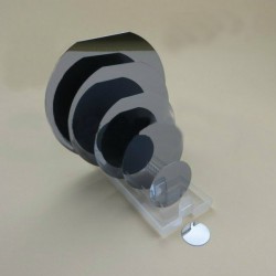
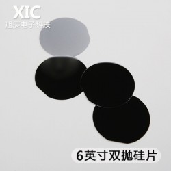
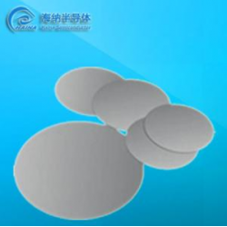
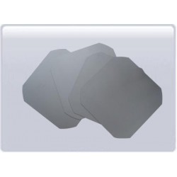
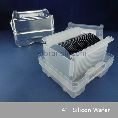
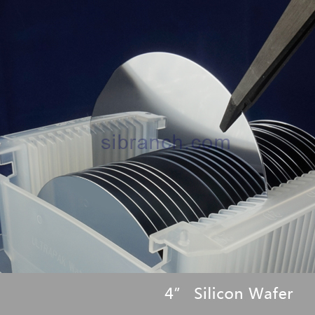
100mm/4" |
| 表面处理 | SSP单面抛光、DSP双面抛光、E/E双面刻蚀、Lapping双面研磨、SiO2/EPI/SOI等 (具体要求详谈) |
| 生长方式 | CZ直拉、FZ区熔 (具体要求详谈) |
| 厚 度 | 100-1000μm (具体要求详谈) |
| 掺杂类型 | P /硼 、N/砷、磷、锑 (具体要求详谈) |
| 晶 向 | <111>/<100> (具体要求详谈) |
| 电 阻 率 | 0.0001-10000(Ω·cm) (具体要求详谈) |
If you have any questions before purchasing, please contact us.

About us | Shopping guide | Business license | Help center | Links | Contact us
Copyright© Semiconductor mall 2015-2016,All Rights Reserved
JingICPPrepare15002921
