 Website Homepage
 Shopping cart
 User center
 Product Category
 inquiry experts experts
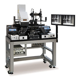


Service Hotline
00864006988696


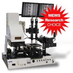
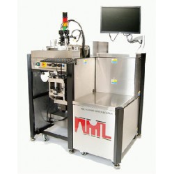
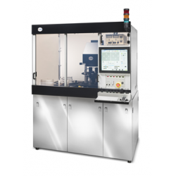
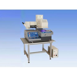
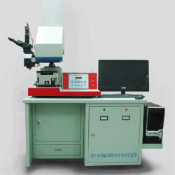
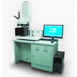
型号6000 FSA用于生产的全自动,上侧或后侧光刻机
用于:半导体,MEMS,传感器,微流体,IOT,包装
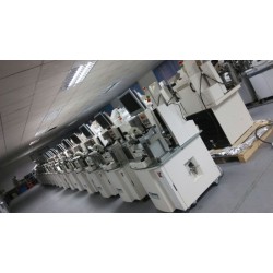
凭借在半导体行业40多年的制造,OAI满足了一个新的精英阶段的生产光刻设备的动态市场的日益增长的挑战。
建立在着名的OAI模块化平台上,6000系列具有完全自动化的亚微米分辨率的顶侧或背侧对齐,提供无与伦比的性价比。
对准器具有先进的光束光学,在第一掩模模式下具有优于±3%的均匀性和每小时180个晶片的吞吐量,这导致更高的产量。 6000系列可以处理厚和粘合基板(高达7000微米),翘曲晶片(高达7 mm-10mm),薄基板(低至100微米厚)和厚光致抗蚀剂的各种晶片。
具有卓越的工艺重复性,6000系列是所有生产环境的完美解决方案。选择顶部或可选的背面对齐,使用OAI的基于Cognex的自定义模式识别软件。对于总体光刻工艺,Series1 6000可以与集束工具无缝集成。 OAI的新生产面罩对齐器是总包。
好处
·全自动
·侧面对齐
•可选:底部对齐
UV到NUV
·集群工具集成
·自定义软件
规格
曝光系统
曝光模式真空接触硬接触软接触接近(2μ间隙)
高级光束
均匀梁尺寸:50mm - 200mm方形/圆
200mm-300mm见方/圆
均匀度:优于±3%
相机:双摄像头与CCTV扩展的景深
对齐系统
模式识别CognexvisionPro¹™与OAI定制软件
对准精度0.5μ顶面
1.0μ,顶部到底部可选背面对齐
预对准精度优于±50μ
自动对齐顶部到底部
顶部
晶片处理
基材尺寸50mm-200mm圆形或方形或200mm-300mm圆形或正方形
薄晶片低至100M
翘曲晶片高达7mm-10mm
厚和粘合基板高达7000μ
机器人单臂和双臂晶片处理
失步补偿标准软件或可选的热卡盘
晶片尺寸转换5分钟以内
吞吐量第一掩模每小时180个晶片 - 随后75-100个晶片每小时
楔形效果平整3点或可选非接触
可用选项
IR自动对齐,
盒式磁带映射
365nm LED曝光光源
温度控制晶片卡盘
集成屏蔽管理控制
用于全光刻的集成光刻集群
使用SMIF或FOUP接口模块的过程环境控制
非接触式调平
边缘夹紧
Model 6000 FSA Fully Automated, Topside or Backside Mask Aligner for Production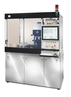
For: Semiconductors, MEMS, Sensors, Microfluidics, IOT, Packaging
With over 4 decades of manufacturing in the semiconductor industry, OAI meets the growing challenge of a dynamic market with a new elite class of production photolithography equipment.
Built on the venerable OAI modular platform, the Series 6000 has topside or backside alignment that is fully automated with sub-micron resolution which delivers performance that is unmatched at any price.
The Aligners have Advanced Beam Optics with better than ±3% uniformity and a throughput of 180 wafers per hour in first mask mode, which results in higher yields. The Series 6000 can handle a wide variety of wafers from thick and bonded substrates (up to 7000 microns), warped wafers (up to 7 mm-10mm), thin substrates (down to 100 micron thick), and thick photo resist.
With superb process repeatability, the Series 6000 is the perfect solution for all production enviroments. Choose either top side or optional back side alignment which uses OAI's customized pattern recognition software that is Cognex based. For the total lithography process, the Seriesl 6000 can be integrated seamlessly with cluster tools. OAI's new production mask Aligners are the total package.
BENEFITS
· Fully Automated
· Topside Alignment
· Optional: Bottomside Alignment
· DUV to NUV
· Cluster Tool Integration
· Customized Software
SPECIFICATIONS
|
|
|
Exposure System |
||||
|
Exposure Modes |
Vacuum contact |
Hard contact |
Soft contact |
Proximity (2μ gap) |
|
Advanced Beam Optics |
||
|
Uniform Beam Size: |
50mm - 200mm square/round |
|
|
|
200mm - 300 mm square/round |
|
|
Uniformity: |
Better than ±3% |
|
|
Camera: |
Dual Camera with CCTV with Expanded Depth of Field |
|
|
Alignment System |
||
|
Pattern Recognition |
Cognex visionPro¹™ with OAI customized software |
|
|
Alignment Accuracy |
0.5μ topside |
|
|
|
1.0μ with top to bottom optional backside alignment |
|
|
Pre-alignment Accuracy |
Better than ±50μ |
|
|
Auto-alignment |
Top to bottomside |
|
|
|
Topside |
|
|
Wafer Handling |
||
|
Substrate size |
50mm – 200mm round or square or 200mm-300mm round or square |
|
|
Thin wafers |
Down to 100Μ |
|
|
Warped Wafers |
Up to 7mm-10mm |
|
|
Thick & Bonded Substrates |
Up to 7000μ |
|
|
Robotics |
Single and dual arm wafer handling |
|
|
Run-out compensation |
Standard software or optional thermal chuck |
|
|
Wafer size conversion |
5 minutes or less |
|
|
Throughput |
1st mask 180 wafers per hour - subsequent 75-100 wafers per hour |
|
|
Wedge Effect Leveling |
3 point or optional non-contact |
|
|
Available Options |
||
|
|
IR Auto-align, |
|
|
|
Cassette Mapping |
|
|
|
365nm LED Exposure Light Source |
|
|
|
Temperature Controlled Wafer Chuck |
|
|
|
Integrated Mask Management Control |
|
|
|
Integrated Lithography Cluster for Full Lithography |
|
|
|
Process Environment Control with SMIF or FOUP Interface Modules |
|
|
|
Non-contact Leveling |
|
|
|
Edge Gripping |
|
If you have any questions before purchasing, please contact us.

About us | Shopping guide | Business license | Help center | Links | Contact us
Copyright© Semiconductor mall 2015-2016,All Rights Reserved
JingICPPrepare15002921
